This article needs additional citations for verification. Please help improve this article by adding citations to reliable sources. Unsourced material may be challenged and removed. Find sources: "Wafer fabrication" – news · newspapers · books · scholar · JSTOR(September 2014) (Learn how and when to remove this message)
Simplified illustration of the process of fabrication of a CMOS inverter on p-type substrate in semiconductor microfabrication. Each etch step is detailed in the following image. Note: Gate, source and drain contacts are not normally in the same plane in real devices, and the diagram is not to scale.
Wafer fabrication is a procedure composed of many repeated sequential processes to produce complete electrical or photonic circuits on semiconductor wafers in semiconductor device fabrication process. Examples include production of radio frequency (RF) amplifiers, LEDs, optical computer components, and microprocessors for computers. Wafer fabrication is used to build components with the necessary electrical structures.
Fabrication Plants
The main process begins with electrical engineers designing the circuit and defining its functions, and specifying the signals, inputs/outputs and voltages needed. These electrical circuit specifications are entered into electrical circuit design software, such as SPICE, and then imported into circuit layout programs, which are similar to ones used for computer aided design. This is necessary for the layers to be defined for photomask production. The resolution of the circuits increases rapidly with each step in design, as the scale of the circuits at the start of the design process is already being measured in fractions of micrometers. Each step thus increases circuit density for a given area.
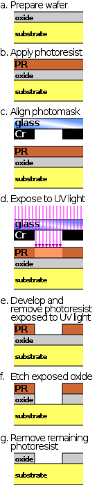
The silicon wafers start out blank and pure. The circuits are built in layers in clean rooms. First, photoresist patterns are photo-masked in micrometer detail onto the wafers' surface. The wafers are then exposed to short-wave ultraviolet light and the unexposed areas are thus etched away and cleaned. Hot chemical vapors are deposited on to the desired zones and baked in high heat, which permeate the vapors into the desired zones. In some cases, ions, such as O2+ or O+, are implanted in precise patterns and at a specific depth by using RF-driven ion sources.
These steps are often repeated many hundreds of times, depending on the complexity of the desired circuit and its connections.
New processes to accomplish each of these steps with better resolution and in improved ways emerge every year, with the result of constantly changing technology in the wafer fabrication industry. New technologies result in denser packing of minuscule surface features such as transistors and micro-electro-mechanical systems (MEMS). This increased density continues the trend often cited as Moore's Law.
A fab is a common term for where these processes are accomplished. Often the fab is owned by the company that sells the chips, such as Intel, Texas Instruments, or Freescale. A foundry is a fab at which semiconductor chips or wafers are fabricated to order for third party companies that sell the chip, such as fabs owned by Taiwan Semiconductor Manufacturing Company (TSMC), United Microelectronics Corporation (UMC), GlobalFoundries and Semiconductor Manufacturing International Corporation (SMIC).
In 2013 the cost of building the next generation wafer fab was over $10 billion.[1]
^Should an Indian fab use older process? Business Standard, 2013
Waferfabrication is a procedure composed of many repeated sequential processes to produce complete electrical or photonic circuits on semiconductor wafers...
finished wafer in a process called die singulation, also called wafer dicing. The dies can then undergo further assembly and packaging. Within fabrication plants...
Retrieved 2023-03-01. "300mm WaferFabrication". 25 December 2010. Archived from the original on 2010-12-25. "200mm WaferFabrication". 25 December 2010. Archived...
105 ha (260 acres), with a main fabrication facility consisting of a 12,000 m2 (130,000 sq ft) 200mm waferfabrication plant. The site is the second-largest...
supplier of wafer-fabrication equipment and related services to the semiconductor industry. Its products are used primarily in front-end wafer processing...
Semiconductor under Amelio chose to build a brand new eight-inch (200 mm) waferfabrication plant in South Portland, Maine. It chose to divest itself of its then...
European Union, and the United States: one 200 mm and one 300 mm waferfabrication plant in Singapore; one 300 mm plant in Dresden, Germany; one 200 mm...
An epitaxial wafer (also called epi wafer, epi-wafer, or epiwafer) is a wafer of semiconducting material made by epitaxial growth (epitaxy) for use in...
Wafer testing is a step performed during semiconductor device fabrication after the back end of line (BEOL) process is finished. During this step, performed...
industry, a semiconductor fabrication plant (commonly called a fab; sometimes foundry) is a factory for semiconductor device fabrication. Fabs require many expensive...
founded in 1993, with the acquisition of National Semiconductor’s 150mm waferfabrication facility in Migdal Haemek, Israel. Tower became a public company in...
technology in the semiconductor industry. Chartered provides comprehensive waferfabrication services and technologies to semiconductor suppliers and systems companies...
silicon wafers even though glass, plastics and many other substrate are in use. Micromachining, semiconductor processing, microelectronic fabrication, semiconductor...
of the United States and initially consisted of two semi-conductor waferfabrication facilities: Fab 10 Ireland Fab Operations (IFO) and also the Fab 24...
headquartered in Shanghai and incorporated in the Cayman Islands. It has waferfabrication sites throughout mainland China, offices in the United States, Italy...
fabrication during which a wafer is prepared for IC packaging and IC testing. The process of die preparation typically consists of two steps: wafer mounting...
microstructures. In August 2002, SMI acquired the IC Sensors' waferfabrication operations and wafer R&D group and relocated to Milpitas, California. The following...
Greenock waferfabrication plant (2019), and Lite-On Semiconductor (2020). On 3 June 2022, Diodes completed the acquisition of the South Portland wafer fabrication...
Wafer bonding is a packaging technology on wafer-level for the fabrication of microelectromechanical systems (MEMS), nanoelectromechanical systems (NEMS)...
IPDs on a silicon substrate are generally fabricated using standard waferfabrication technologies such as thin film and photolithography processing. For...
2022, Texas Instruments broke ground on new 300-mm semiconductor waferfabrication plants in Sherman, Texas, and projected its investments will reach...
semiconductor wafer processing equipment for the fabrication of semiconductor devices. ASM's products are used by semiconductor manufacturers in front-end wafer processing...
uses external suppliers for all phases of manufacturing, including waferfabrication, assembly, testing, and packaging. Nvidia thus avoids most of the...
Ventures. The company develops and manufactures equipment used in the waferfabrication steps of creating a semiconductor device, including atomic layer deposition...
September 2012). Production Planning and Control for Semiconductor WaferFabrication Facilities: Modeling, Analysis, and Systems. Springer Science & Business...
How Silicon Chips Are Made article on TechRadar Wafering - By SolarWorld USA Silicon WaferFabrication Process - By the Department of Electrical and Computer...
 Global Information