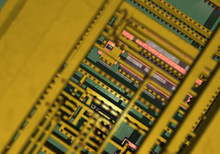
Synthetic detail of a micromanufactured integrated circuit through four layers of planarized copper interconnect, down to the polysilicon (pink), wells (greyish) and substrate (green)
Microfabrication is the process of fabricating miniature structures of micrometre scales and smaller. Historically, the earliest microfabrication processes were used for integrated circuit fabrication, also known as "semiconductor manufacturing" or "semiconductor device fabrication". In the last two decades microelectromechanical systems (MEMS), microsystems (European usage), micromachines (Japanese terminology) and their subfields, microfluidics/lab-on-a-chip, optical MEMS (also called MOEMS), RF MEMS, PowerMEMS, BioMEMS and their extension into nanoscale (for example NEMS, for nano electro mechanical systems) have re-used, adapted or extended microfabrication methods. Flat-panel displays and solar cells are also using similar techniques.
Miniaturization of various devices presents challenges in many areas of science and engineering: physics, chemistry, materials science, computer science, ultra-precision engineering, fabrication processes, and equipment design. It is also giving rise to various kinds of interdisciplinary research.[1] The major concepts and principles of microfabrication are microlithography, doping, thin films, etching, bonding, and polishing.
Simplified illustration of the process of fabrication of a CMOS inverter on p-type substrate in semiconductor microfabrication. Each etch step is detailed in the following image. Note: Gate, source and drain contacts are not normally located in the same plane in real devices, and thus, the diagrams are not to scale.Detail of an etch step.
^Nitaigour Premchand Mahalik (2006) "Micromanufacturing and Nanotechnology", Springer, ISBN 3-540-25377-7
Microfabrication is the process of fabricating miniature structures of micrometre scales and smaller. Historically, the earliest microfabrication processes...
Three-dimensional (3D) microfabrication refers to manufacturing techniques that involve the layering of materials to produce a three-dimensional structure...
high but lateral etch-rate is very small, are essential processes in microfabrication of integrated circuits and MEMS devices. An isotropic antenna is an...
photolithographic cycle as many as 50 times. It is also an important technique for microfabrication in general, such as the fabrication of microelectromechanical systems...
Integrated circuit packaging is the final stage of semiconductor device fabrication, in which the die is encapsulated in a supporting case that prevents...
(BOE), also known as buffered HF or BHF, is a wet etchant used in microfabrication. Its primary use is in etching thin films of silicon dioxide (SiO2)...
etching techniques (such as deep reactive-ion etching) are used in microfabrication processes to create well defined microscopic features with a high aspect...
suggests, microelectronics relates to the study and manufacture (or microfabrication) of very small electronic designs and components. Usually, but not...
see today. Microelectronics engineering deals with the design and microfabrication of very small electronic circuit components for use in an integrated...
molecular biology, semiconductor physics, energy storage, engineering, microfabrication, and molecular engineering. The associated research and applications...
CollinsWillow, 1996. page 206. Madou, Marc J (2002). Fundamentals of Microfabrication. Taylor & Francis. ISBN 0-8493-0826-7. Roth, Leland M (1993). Understanding...
to indium phosphide in microfabrication to etch silicon nitride selectively with respect to silicon dioxide in microfabrication to etch aluminium as a...
hydroxide. This process is used in texturing of silicon solar cells and microfabrication (e.g. in MEMS devices). Isopropyl alcohol increases the anisotropy...
fabrication of a CMOS inverter on p-type substrate in semiconductor microfabrication. In step 1, silicon dioxide layers are formed initially through thermal...
383–391. Retrieved 16 October 2008. Madou, M.J. (2002). Fundamentals of Microfabrication: the Science of Miniaturization (2nd ed.). CRC Press. pp. 53–54....
creating regions of increased or decreased conductivity) Etching (microfabrication) Dry etching (plasma etching) Reactive-ion etching (RIE) Deep reactive-ion...
space and terrestrial power systems. Research in nanotechnology and microfabrication is conducted by the Nano and Micro Devices Center. Atmospheric Sciences...
field-effect transistors. Using carbon nanotubes as a scaffold for diverse microfabrication techniques. Energy dissipation in self-organized nanostructures under...
fabrication of a CMOS inverter on p-type substrate in semiconductor microfabrication. Each etch step is detailed in the following image. Note: Gate, source...
(a) Schematic representation of a masking microfabrication process. After creating a monolayer of fluorescent particles, bilayers of 1:10 Ti/Au are deposited...
tb04289.x. Johansson S, Schweitz JÅ, Westberg H, Boman M (1992). "Microfabrication of three-dimensional boron structures by laser chemical processing"...
 Global Information