Thin-film deposition technique that deposits one 1-atom thick layer at a time
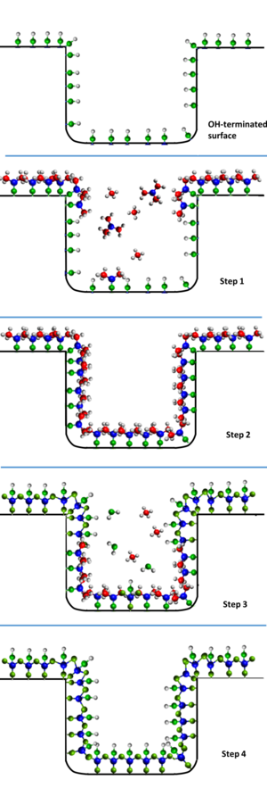
Schematic illustration of one reaction cycle of the ALD process, using the trimethylaluminium (TMA) -water process to make thin aluminium oxide films as (simplified) example. There, the starting surface contains hydroxyls (OH groups) as reactive sites; Step 1 is the reaction of TMA; Step 2 is a purge or evacuation step, Step 3 is the reaction of water, and Step 4 is a purge or evacuation step. Image in Wikimedia Commons (CC BY 4.0 licence), first published in https://doi.org/10.1063/1.5060967 (Copyright Authors, CC BY 4.0 licence).
Atomic layer deposition (ALD) is a thin-film deposition technique based on the sequential use of a gas-phase chemical process; it is a subclass of chemical vapour deposition. The majority of ALD reactions use two chemicals called precursors (also called "reactants"). These precursors react with the surface of a material one at a time in a sequential, self-limiting, manner. A thin film is slowly deposited through repeated exposure to separate precursors. ALD is a key process in fabricating semiconductor devices, and part of the set of tools for synthesizing nanomaterials.
and 23 Related for: Atomic layer deposition information
Atomiclayerdeposition (ALD) is a thin-film deposition technique based on the sequential use of a gas-phase chemical process; it is a subclass of chemical...
fabrication plants. ASM's technologies include atomiclayerdeposition, epitaxy, chemical vapor deposition and diffusion. The company was founded by Arthur...
Essentially, MLD resembles the well established technique of atomiclayerdeposition (ALD) but, whereas ALD is limited to exclusively inorganic coatings...
Many growth methods rely on nucleation control such as atomic-layer epitaxy (atomiclayerdeposition). Nucleation can be modeled by characterizing surface...
(2014-12-01). "A Short History of AtomicLayerDeposition: Tuomo Suntola's AtomicLayer Epitaxy". Chemical Vapor Deposition. 20 (10–11–12): 332–344. doi:10...
reactions underpinning the thin film deposition technique that years later became known as atomiclayerdeposition. He was the rector of Leningrad Technological...
created using atomiclayerdeposition (ALD) with unique physical, chemical, and electronic properties. For example, a rough oxide layer can be further...
of. CVD is extremely useful in the process of atomiclayerdeposition at depositing extremely thin layers of material. A variety of applications for such...
a thin film is a prerequisite and the preferred growth mode is atomiclayerdeposition, Al2O3 films can be prepared by the chemical exchange between trimethylaluminium...
University of Connecticut are using a technique called selective area atomiclayerdeposition that is capable of producing them reliably and at industrial scales...
materials science, developing the thin film growth technique called atomiclayerdeposition. Suntola was born in Tampere, Pirkanmaa, in 1943, during the Continuation...
evaporation (e.g. CrBO3, β‐BaB2O4), pulsed laser deposition (e.g. β‐BaB2O4, Eu(BO2)3), and atomiclayerdeposition (ALD). Growth by ALD was achieved using precursors...
TiO2 layerdeposition be compatible with flexible polymer substrate, low-temperature techniques, such as atomiclayerdeposition, molecular layer deposition...
Department of Energy's Argonne National Laboratory. He leads Argonne's atomiclayerdeposition (ALD) research program, where he directs research and development...
Layer-by-layer (LbL) deposition is a thin film fabrication technique. The films are formed by depositing alternating layers of oppositely charged materials...
electrochemical deposition (ECD) and chemical vapor deposition (CVD) technologies to form copper and other metal films for conducting structures. Atomiclayer deposition...
Sputter deposition is a physical vapor deposition (PVD) method of thin film deposition by the phenomenon of sputtering. This involves ejecting material...
computers." The IEEE states: "Sandhu initiated the development of atomiclayerdeposition high-κ films for DRAM devices and helped drive cost-effective implementation...
focused ion beam machining, nanoimprint lithography, atomiclayerdeposition, and molecular vapor deposition, and further including molecular self-assembly...
(CVD) Metal organic chemical vapor deposition (MOCVD), used in LEDs Atomiclayerdeposition (ALD) Physical vapor deposition (PVD) Sputtering Evaporation Epitaxy...
chemical vapor deposition or atomiclayerdeposition. The Al2O3 provides excellent surface passivation of p-doped silicon surfaces. The Al2O3 layer is typically...
 Global Information